

China intensifies efforts to develop its own advanced semiconductor lithography capabilities by 2030, as explained by Nvidia’s Jensen Huang, indicating a significant technological shift.
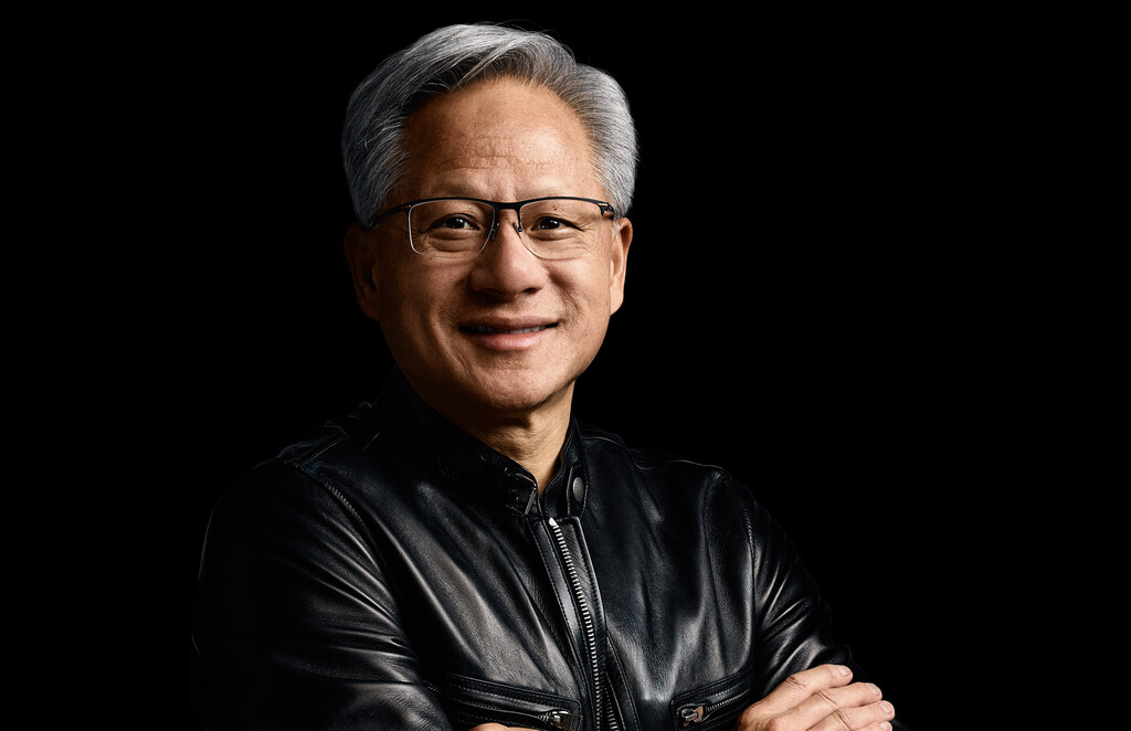
Jensen Huang, CEO of Nvidia, has shared a bold vision for China’s technological future, forecasting that the country will have advanced lithography machines by 2030. Speaking on The All-In Podcast, Huang emphasized the inevitability and impending reality of China’s ascension in this domain. Such statements hold weight, given Huang’s position and the significant strides China is making in semiconductor technology.
Progress in Photolithography
China’s effort to become self-reliant in semiconductor manufacturing has been a driving force behind state-backed projects. Recent reports highlight China’s advancements in producing immersion deep ultraviolet (DUV) lithography machines, an essential step towards autonomous chip production. Although the specific company achieving this feat remains undisclosed, it’s likely that Huawei-affiliated Shanghai Yuliangsheng Technology is leading this innovation.
The development of these machines marks a significant milestone. For years, China has struggled to domestically produce these critical tools, which are pivotal in engraving circuit patterns on silicon wafers. The successful creation of such equipment not only underscores China’s technological ingenuity but also its strategic pivot to lessen dependence on foreign technology.
State-Endorsed Technological Projects
China’s commitment to leading the semiconductor race is evident through extensive governmental support. Companies like SiCarrier, Shanghai Micro Electronics Equipment (SMEE), and Huawei have received lucrative subsidies to foster development in UV photolithography. The strategic intent is clear: establish a robust local supply chain to produce cutting-edge semiconductors without relying on external manufacturers like ASML.
Two flagship projects emerge as cornerstones of this endeavor. The first involves Huawei testing a domestically designed extreme ultraviolet (EUV) lithography machine. This prototype distinguishes itself by using an LDP (laser-induced plasma) light source, reputedly more straightforward to implement than the LPP counterparts employed by ASML. Though still in the development stage, such innovations hint at a transformative capability shift in China’s semiconductor production industry.
Next Generation: The SSMB-UVE Approach
SSMB-UVE introduces a novel approach to generating high-energy UV radiation, utilizing a synchrotron—a particle accelerator typically used in atomic-level research. This project, spearheaded by the University Tsinghua and the Chinese Academy of Sciences, aims to power surrounding semiconductor fabrication plants, akin to how power stations supply electricity. While practical applications might be years away, the project’s potential impact could reshape semiconductor manufacturing paradigms.
Detected Pattern: Infrastructure Shift
The advancements in lithography technology highlight an ongoing infrastructure shift in the global semiconductor landscape. China’s pursuit of self-sufficiency represents a strategic move to secure its position in the technological hierarchy and mitigate geopolitical dependencies. By 2030, if successful, China’s lithography capabilities could redefine global supply chains, offering a new alternative to existing monopolies in the industry.
This infrastructural evolution signals broader implications for international relations, economic strategies, and technological sovereignty, potentially altering the dynamics within the AI and automation sectors. As these developments unfold, monitoring and understanding these shifts remains crucial for stakeholders worldwide.
While the road to 2030 remains lined with challenges, China’s concentrated efforts suggest a determined trajectory towards achieving advanced semiconductor capabilities. Monitoring continues.