
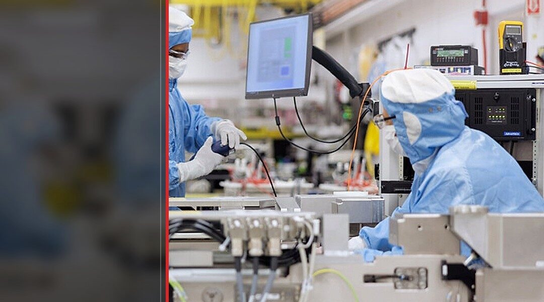
Ultraviolet lithography tech, used in chip-making, now shows potential to inscribe ‘The Lord of the Rings’ on a paper edge, demonstrating its precision.
The potential to write J.R.R. Tolkien’s ‘The Lord of the Rings’ on the edge of a paper sheet exemplifies the extraordinary precision of technology, initially developed for chip fabrication. The machines behind this feat, ultraviolet extreme (UVE) lithography devices, are from the Netherlands-based ASML, a pioneering entity in semiconductor manufacturing.
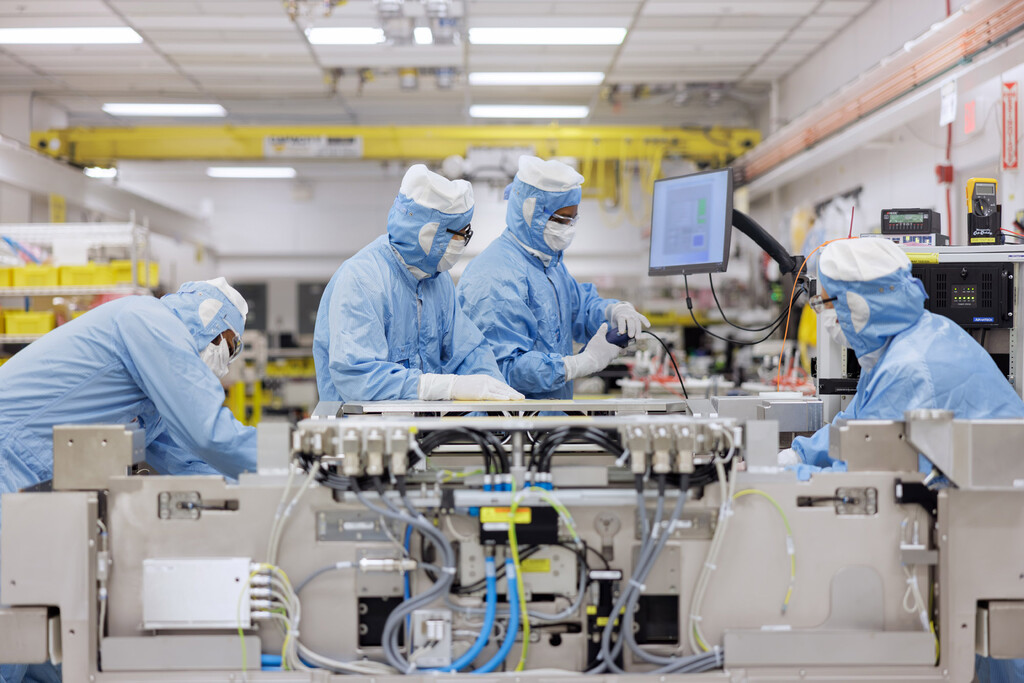
Initially, the functionality of these machines seemed unachievable. In 1997, however, a shift occurred when ASML’s research leader, Jos Benschop, identified the viability of using UVE technology. Partnering with Zeiss, a German company capable of crafting sophisticated mirrors, they laid the groundwork for modern circuits in smartphones, computers, and AI servers.
Ultraviolet Precision
These devices utilize ultraviolet light with incredibly short wavelengths—specifically 13.5 nm to avoid materials that pose toxic hazards like berilium. This specific wavelength is a delicate choice made by engineers aiming to circumvent materials that had adverse properties when exposed to shorter wavelengths. The employment of molybdenum and silicon, elements safe for use in UVE devices, is fundamental to this technological marvel.
“13.5 nm is more than just a number; it’s the cornerstone of modern precision in technology,” remarked Martin van den Brink, a key figure in ASML’s technological advancements.
The Journey from UVE to Beyond
ASML’s UVE technology is not static. The company is progressing toward Hyper-NA photolithography machines, maintaining the 13.5 nm wavelength but enhancing resolution through improved optical aperture values. These advancements promise even greater precision, expected to debut by 2033, confirming the enduring relevance of UVE technology.
Currently, industry leaders such as TSMC, Intel, and Samsung are embedding these machines into their production lines. These businesses benefit from UVE lithography’s enhanced capabilities, marking a pivotal shift in technology infrastructure.
System-Level Shift: Analyzing Workflow Compression
The precision of ASML’s machines automates complex manufacturing tasks, shifting human reliance from manual oversight to technological processes. This automation compresses workflows, streamlining operations and minimizing human intervention. In AI and chip production, workflow compression reduces production time, enhances output quality, and lowers error rates.
This not only transforms manufacturing processes but also sets precedents across various sectors reliant on precision and efficiency. The compression of workflows facilitated by UVE technology represents a significant evolution in both the AI and broader technological landscape.
Implications for AI and Beyond
The impact of ASML’s innovations transcends chipmaking. The precision technology holds potential implications for AI development, where data processing and hardware capabilities are critical. Workflow compression, enabled by these machines, may lead to faster and more efficient AI systems, bolstering development cycles and performance metrics.
Moreover, the potential to miniaturize data inscriptions, as illustrated by the ‘LOTR’ analogy, demonstrates strategic advancement in data storage solutions, contributing to more sophisticated AI models and analytics infrastructure.
ASML’s UVE technology reflects more than advanced chip manufacturing; it exemplifies a shift towards automated precision across various industries. As Hyper-NA machines prepare for market entry, we anticipate not only continued influence in semiconductor production but also broader technological transformations. Monitoring continues.